Saike 858D Rework Station - Original Schematic
Recently, I posted the teardown of my Saike 858D SMD rework station. Now it is time to really reverse engineer the main PCB. Some of the parts are similar to other “flavors” of the 858D, but some seem to be different.
Approach
My process of reverse engineering can be seen in the following picture (click for large version).
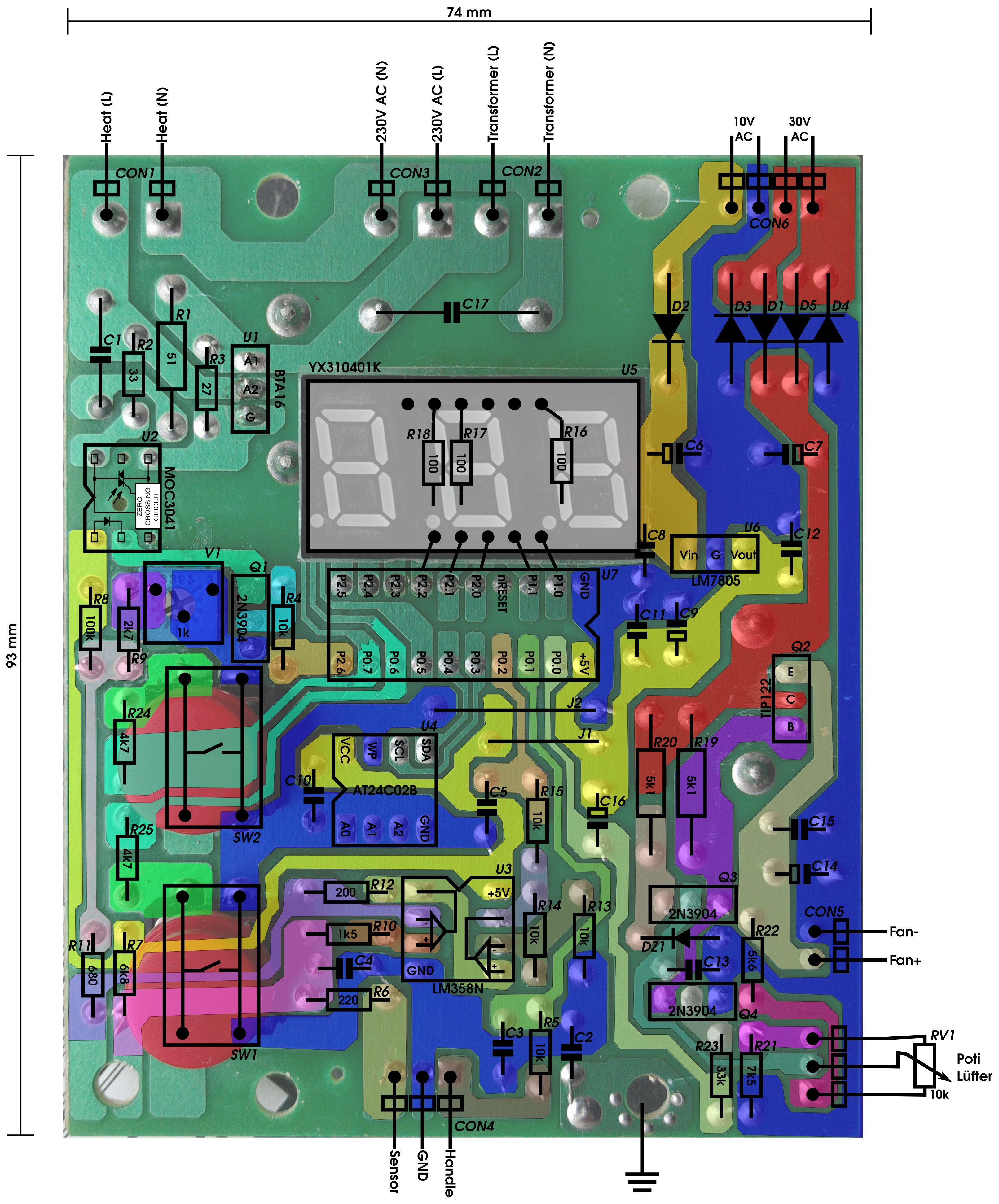
I started with a picture of the copper side of the PCB which I flipped horizontally, so this view is kind of an “X-Ray” view through the front side of the PCB.
Then I started with marking most of the copper traces in different colors. Most of the colors are just randomly chosen, but the yellow area is the +5V VCC line and the 0V areas are marked blue.
Afterwards I added all the components on a second layer. Due to the mirrored back side graphics, I can match the position to the image of the front side of the PCB and still read parts numbers.
Lastly, I added all part references and as much part information as possible, i.e. part names, pin names, etc. I took the values from resistors from their marking visible on the images. However I am not entirely sure that all values are correct, because at some places I have the nagging feeling that the values are not matching my expectations.
Schematics
I rebuilt the schematics of the PCB in KiCad. Here is the complete schematic in all it’s glory.
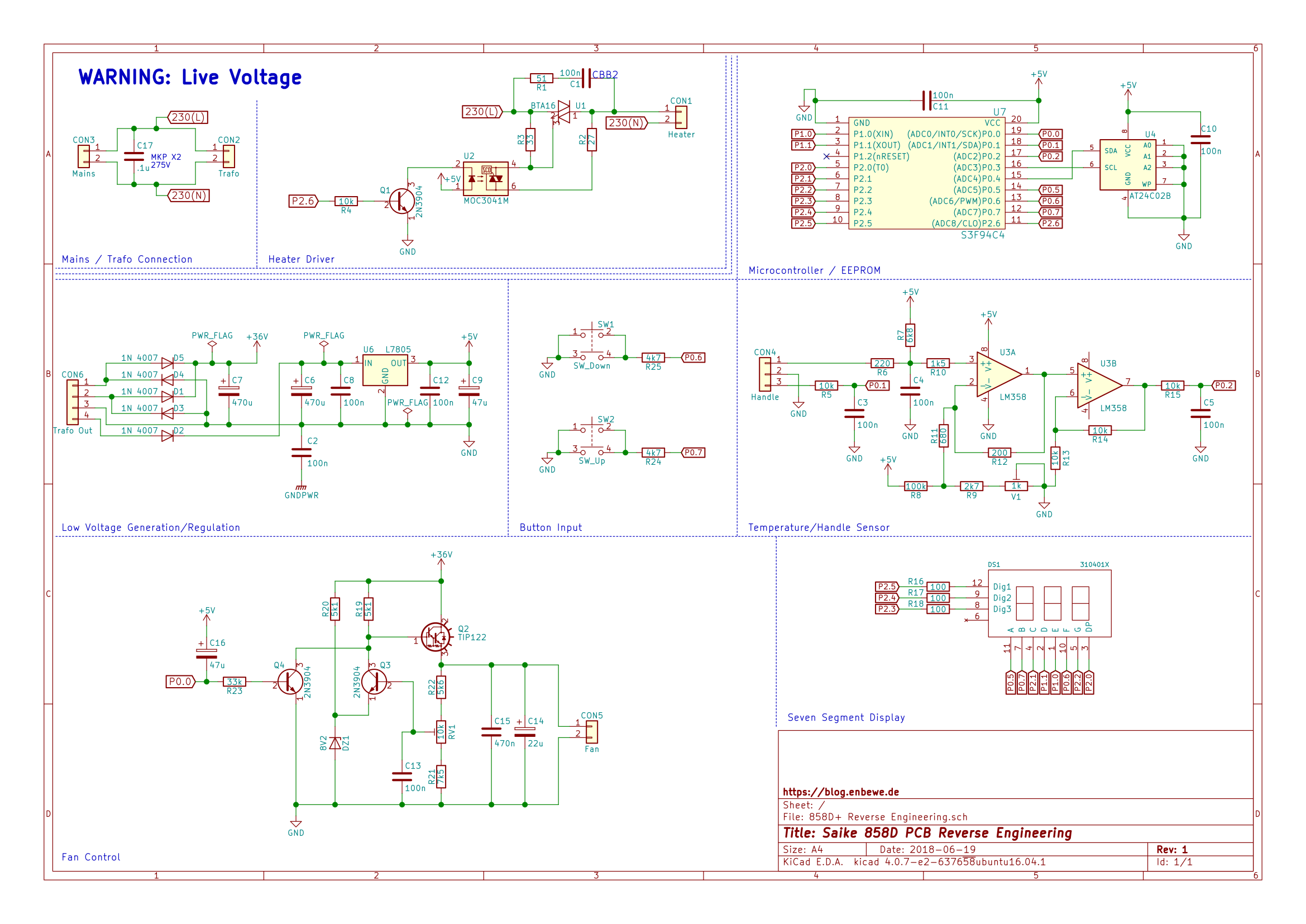
Let’s go through the parts one by one. We start at the top left and continue in normal reading direction.
Mains connection and Heater driver
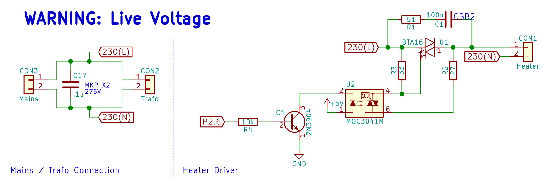
The left part of the schematic is about as simple as possible. The mains power is bridged over to the connector for the transformer. The only notable part is a big suppression capacitor (0.1uF 275V) by Tenta.
The right part of the schematic is the heater control circuit. The microcontroller can control the NPN-transistor Q1 through the limiting resistor R4. This pulls down the cathode potential and activates the optocoupler U2 which is a MOC3041. The MOC3041 is a triac driver and that it does. It contains a zero-crossing detection circuit and controls the triac U1, which in my device is a BTA16. The additional circuitry is pretty much the recommended design from the MOC3041 datasheet. However, the resistor values for R2 and R3 seem a bit low. The datasheet suggests 360 and 330 Ohms for these resistors.
Microcontroller and EEPROM
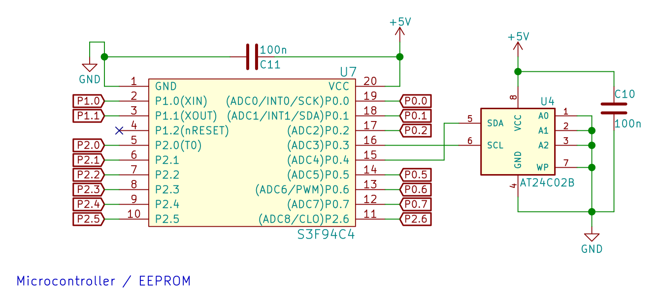
No surprises here. One capacitor just for supply stability and that’s it. The microcontroller has no EEPROM integrated, which leads to an additional EEPROM chip on the PCB. For some reason it is not connected to the dedicated SDA/SCK pins on the microcontroller. The EEPROM memory is hard-wired to address 0 by tying all address pins to ground.
Voltage Regulation
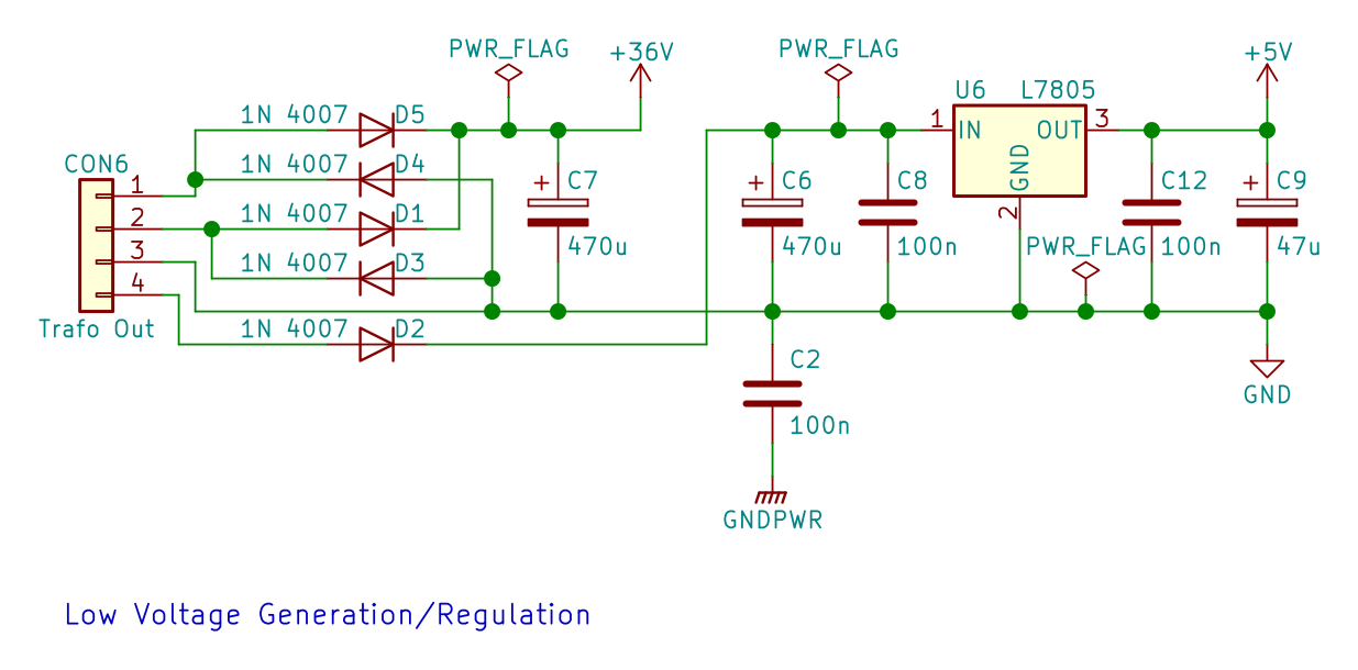
Just a pretty standard power supply desing. The connector carries the two outputs from the transformer, 30VAC on pin 1 and 2 and 10VAC on pin 3 and 4.
The 30V rail is rectified using a full bridge rectifier and C7 as a smoothing capacitor. The resulting voltage should be about 40V but the 36V power net is the closest value I had in KiCad.
The 10V rail is half bridge rectified through D2 and smoothed with C6. Afterwards, the 7805 voltage regulator creates a stable 5V supply for the logic components.
The common 0V net is connected to the protective ground of the casing through capacitor C2.
Buttons
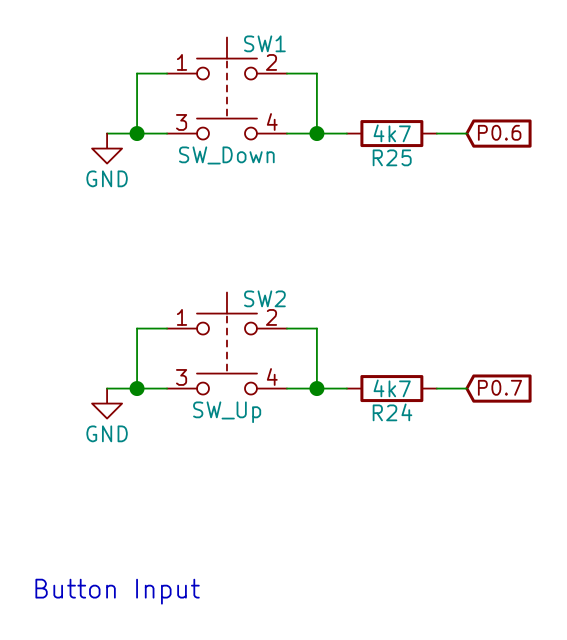
This one doesn’t really justify its own part. The buttons are connected to ground and pull their respective logic line down when they are closed. R24 and R25 are used to limit the current.
The pins used on the microcontroller for the buttons are also used to drive the display. I guess there is sufficient time in between the display control to read the logic state from the buttons.
Handle and Temperature Sensor

This one is the one I have the most problems with for now. Let’s start with the reed sensor which comes in through pin 3 of CON4. The signal is just filtered through R5 and C3 and fed to the microcontroller.
The temperature sensor is more of an issue and I havn’t fully understood the whole thing yet. R15 and C5 are again a filter like for the reed sensor. U3B, R13 and R14 form a basic non-inverting amplifier circuit with a gain of 2. The other operational amplifier, together with V1, R8, R9, R11, and R12, probably forms some non-inverting amplifier with an offset voltage. For now I didn’t really understand the design. R6 and C4 form another filter on the input side of the amplifier. R7 provides some kind of offset in the signal, but I currently have no real idea why that is done.
Fan Control
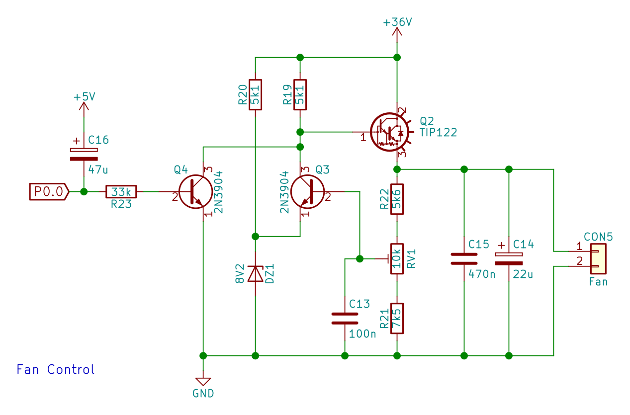
This circuit I didn’t understand at first, but Christean’s work put me on the right track.
The fan is controlled through transistor Q2. The fan is rated for 24V, but the supply voltage is a bit more than 40V. The circuit has to make sure that the fan is not overloaded. The microcontroller can use transistor Q4 to drain the base current of Q2 and turn the controller off this way. If Q2 is turned off, the speed control is implemented through Q3 and the surrounding circuit. The more Q3 is conducting, the more the base current is drained and the less Q2 is conducting. However, Q3 cannot drain Q2 completely, as the emitter voltage of Q3 always sits one diode drop above ground level.
RV1, which is the front-panel potentiometer, can be used to control the voltage divider between R21 and R22. The higher the voltage at the taper of the potentiometer, the higher the base current of Q3, resulting in less conductance for Q2. In addition the voltage divider and the transistor form a feedback loop to control the base current of Q2, and in result the voltage on the fan.
LCD Display
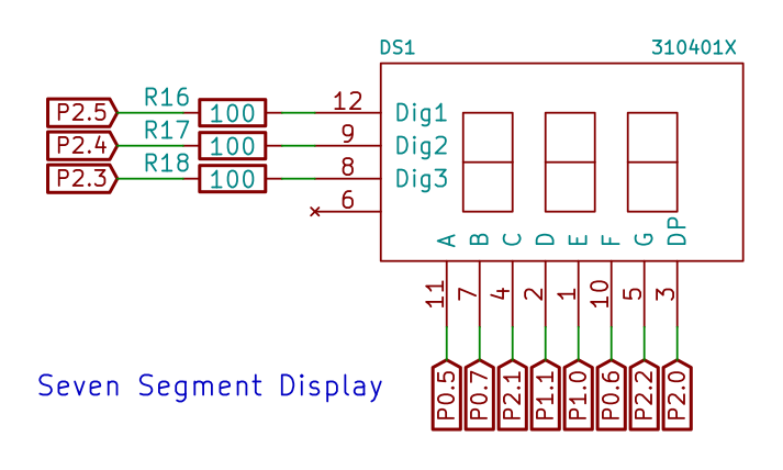
The display is a three digit, seven-segment display with decimal points. The segments are wired with a common anode. The three digits activated one by one and rely on persistence of vision to show a stable image.